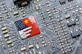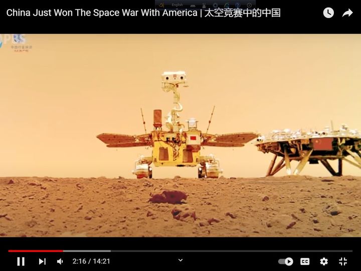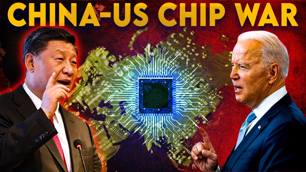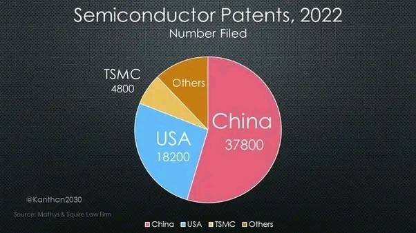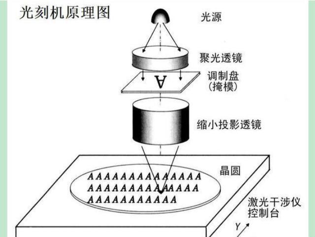


UDN says in November, 2022 Huawei has applied for the patent of ultraviolet EUV lithography scanner. Application Number was 202110524685. It covers all crucial components of an EUV scanner including a 13.5 nm EUV light generator (light source), a set of reflecting mirrors, the lithographic system and control management technologies. This will help Chinese chip making companies to produce below 7 nm chips. This is a great victory for China and Huawei against the Semiconductor War unleashed by USA. Dutch EUV scanner maker ASML was forced not to sell EUV to Chinese companies. ASML has to abide by US order as it uses many US technologies in its production line. Moreover, ASML is only company in the world making lithographic EUV scanner. But is has taken financial help from Intel, Micron, HKHynix, Samsung and TSMC. So ASML is bound to give EUV scanner to these companies. But ASML has no obligation to give EUV scanner to any Chinese company. USA used this opportunity and denied ASML EUV scanner to Chinese semiconductor making industry.
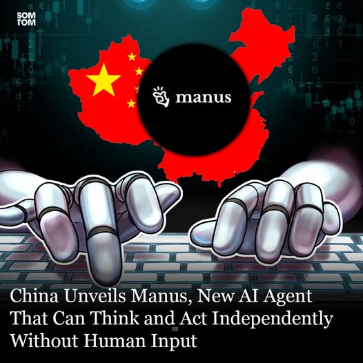
Huawei and Chinese Academy of Sciences agreed that making ultraviolet EUV lithography scanner domestically is the key to break US seize of Chinese semiconductor making industry. Huawei is world's biggest cooperative company with USD 100 billion revenue. It set chip production and wafer fab equipment (wfe) production as its primary objectives. Huawei and HiSkey have top notch chip design skills but that is useless without EUV scanner. So Huawei started to invest in EUV scanner production.
Chinese actions soon started giving excellent results. Huazhao Precision Tech developed dual stage system, only second company after ASML to do so. Watching this development ASML warned USA that China will be able to produce EUV scanner in 15 years if the ban continues. But China made more progress in just 1 year. Professor Tang Chuanxiang of Tsinghua University succeeded in exploring a new type of particle accelerator light source "stead state micro bouncing" in February, 2022. This can be used in EUV production as well as in other high tech industries. By August, 2022, Chinese Academy of Sciences has officially completed the installation and application of high energy radiation light source equipment. At the same time, the linear Lloyd lens coating device and nano-focusing lens coating device developed by Zhongke Kemei have also been put into use. These two devices combined with high-radiation light source equipment can almost meet the physical lens technology of all process requirements, including Zeiss lenses.
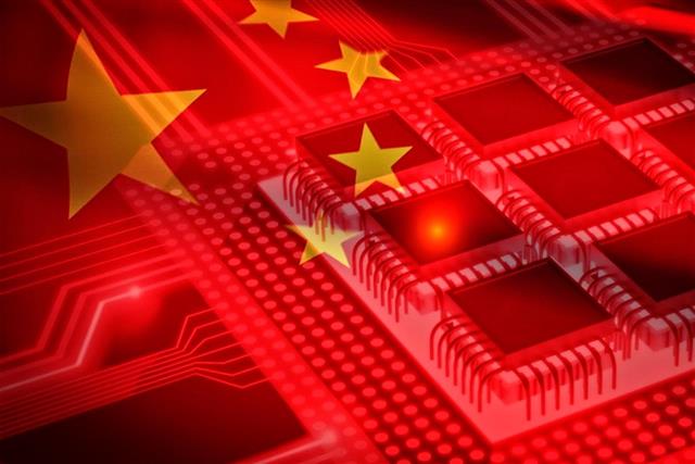
This means that the three core technologies of EUV lithography machines namely the dual work stage system, the light source and the optical lens have all been broken. But we must remember that filing patent is completely different from actual production because actual production needs to tackle lot of practical problems. Moreover, even with EUV scanner chip making is not possible if there is no pellicle of masks, resists, etc.
Author: Saikat Bhattacharya